About this product
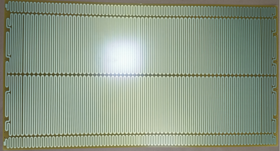
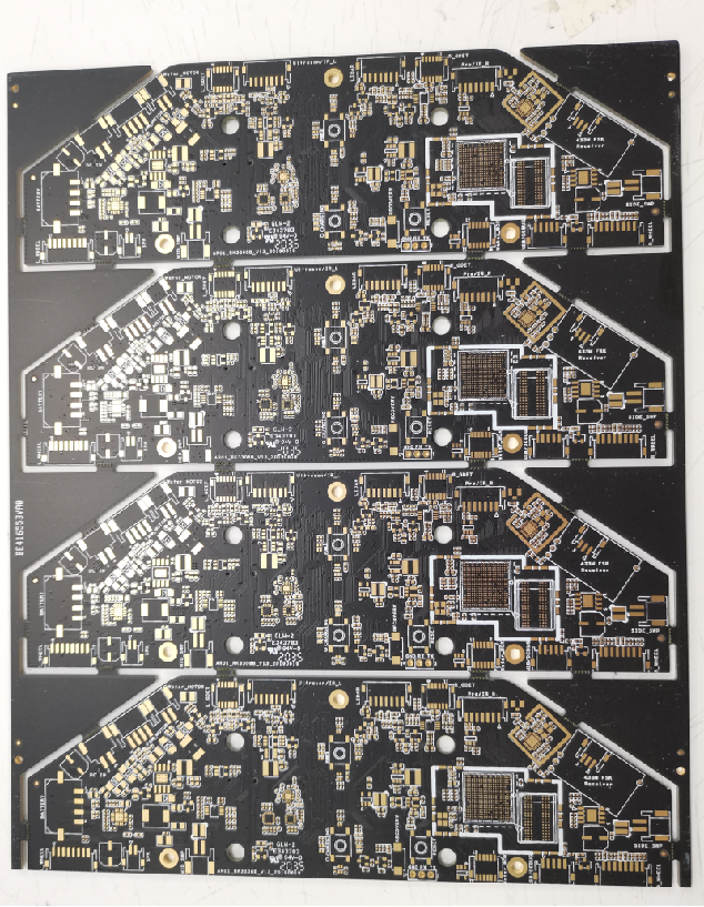
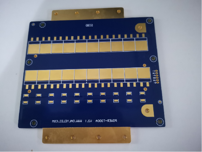
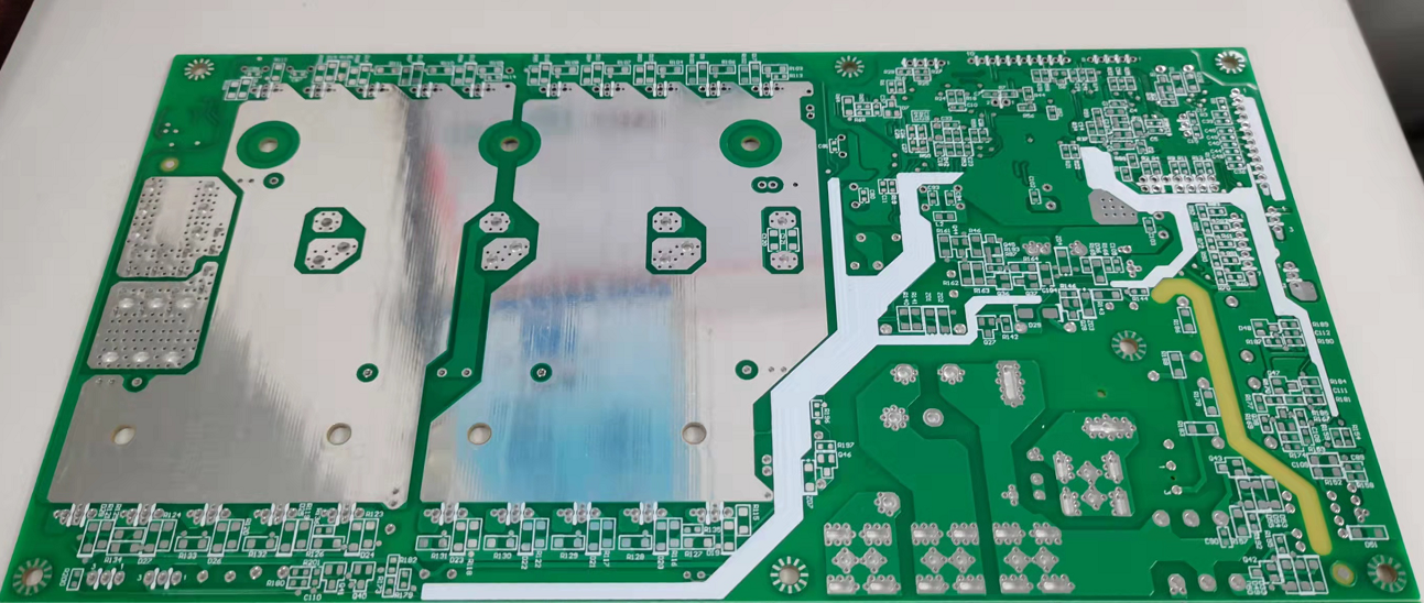
This listing details advanced Printed Circuit Board (PCB) Manufacturing Processes, encompassing both subtractive and semi-additive methodologies crucial for modern electronics production. These processes are designed to precisely etch and build conductive pathways onto insulating substrates, forming the backbone of virtually all electronic devices. Key features include high precision etching capabilities, controlled material deposition, and advanced photolithography techniques, ensuring the creation of complex and miniaturized circuit designs with exceptional signal integrity. The construction quality relies on robust industrial-grade equipment and meticulously controlled chemical baths, with finishes optimized for solderability and environmental resistance. While specific size ranges are dependent on the final PCB design, these processes are adaptable to a wide spectrum of board dimensions and layer counts. Typical applications span the entire electronics industry, from consumer electronics and telecommunications to automotive, aerospace, and medical devices. Target buyers include PCB manufacturers, electronics assembly houses, contract manufacturers, and large-scale importers and wholesalers seeking to integrate advanced PCB fabrication capabilities into their supply chains. These processes are fundamental to achieving industry-standard PCB quality and performance, making them essential for international trade buyers looking to source high-quality electronic components.